Dual gate material (Au and Pt) based double-gate MOSFET for high-speed devices
Naveenbalaji Gowthaman1, Viranjay M. Srivastava2
Gowthaman, N; Srivastava, V.M. Dual gate material (Au and Pt) based double-gate MOSFET for high-speed devices. Tecnología en Marcha. Vol. 34, especial. Noviembre LAEDC 2021. Pág 10-16. https://doi.org/10.18845/tm.v34i6.5966
Keywords
Double-gate MOSFET; high-speed devices; high-k dielectric; microelectronics; nanotechnology; VLSI.
Abstract
Aluminium Gallium Arsenide (AlGaAs) is a semiconductor material used in the latest design of double heterostructure laser diodes. This semiconductor is mostly available in the arbitrary alloy form between Gallium Arsenide and Aluminium Arsenide. It is derived from the Tri-Methyl-Gallium (TMG/TMGa), and Arsine (AsH3), both the chemicals are pyrophoric and toxic. The resistance is less between source and drain contacts in the case of AlGaAs so that it has been proposed as a material to grow contacts on Indium Phosphide (InP) layer. The AlGaAs uses an ion implantation model for a design purpose which lowers the thermal power while the operation of the device. The parasitic capacitance has to be taken care of while designing a device using this material since the capacitance affects much in the AlGaAs based devices. The average velocity of the electrons has been observed to be increased by 14.63 % in the Au-gate (gate-1) and Pt-gate (gate-2) material-based Double-Gate (DG) MOSFET compared to the Silicon-based DG MOSFET. This paves the way for higher electron mobility, in turn, it can be used in high-frequency device manufacturing. The proposed material can be used in high-speed hybrid applications such as HEMTs and radiofrequency devices for long-haul communication.
Introduction
Gallium Aluminium Arsenide (AlGaAs), a semiconductor material that has electrical properties near the Gallium Arsenide (GaAs). The AlGaAs has a similar lattice constant to the GaAs but has a wider bandgap, making them compatible for designing high-speed devices. Usually, this material available in arbitrary alloy form, which depends on the x value, material stays between the Gallium Arsenide (GaAs) and Aluminium Arsenide (AlAs). The value of x mainly impacts the alloy’s bandgap, such as x < 0.4 makes the direct bandgap. The GaAs have a bandgap of 1.42 eV and AlAs has a bandgap of 2.16 eV. Hence, Gallium Aluminium Arsenide can be used as a barrier in the Gallium Arsenide bulk [1]. This makes the heterostructures more reliable for high-speed applications. The application areas are semiconductor lasers and optoelectronic devices for long-distance wireless communications [2]. This device has been used to construct Quantum Well Infrared Photo (QWIP) detector because Aluminium Gallium Arsenide has higher stability in a lower power budget than GaAs.
Hill et. al. [2] had presented an enhancement-mode MOSFET which is based on III-V semiconductors with gate and insulator layer with metal and high-k-dielectric respectively with the greater mobility of electrons and improved transconductance. These mobility and device parameters are highly suitable for future design of n-channel CMOS transistors and High Electron Mobility Transistors (HEMTs) based on III-V semiconductor MOSFETs. Sen et. al. [3] had demonstrated a detailed analysis of the parameters of AlxGa1-xAs/GaAs junction-less Double-Gate (DG) MOSFET form of sensitive biosensor application modules. Allaei et. al. [4] had proposed an extensive and analytic charge-based model for measuring the Short Channel Effects (SCEs) in Gallium Nitride based MOSFETs. Liu et. al. [5] stated Technology CAD models and their detailed analysis for AlGaAs/InGaAs; AlGaN/GaN, and Silicon-On-Insulator TeraFETs are in good agreement with the obtained current-voltage parametrs and the response to the sub Tera-Hz radiation. Hence, the DG-MOSFETs can be designed using AlGaAs material. This paper has been organized as follows. Section II elaborates the design process and its parametric model. Section III has the result and discussion of the proposed model. Finally, Section IV concludes the work and recommends the future aspects.
Infinitesimal Design Model
Wide research has been in the long run to make MOSFETs with advanced dielectric materials with higher k – Kappa value to reduce the SCEs. The scaling down of device models has been developed with high-k dielectric materials grown on the well between the gate contacts. Previously SiO2 layer was used as an insulator between gate material and channel [6, 7]. The usage of high k dielectric makes more insights into research in device fabrication [8, 9]. The Gold and Platinum gate material has been used to construct DG MOSFETs as shown in figure 1. The average electron velocity is higher than the previously discussed model in [5]. The material’s total length has been fixed to 30 nm from the source and drain along with the entire electronic simulation [8-10]. The material behaves faster than the previous average velocity [5, 11, 12]. The drain current as in equation (1) of the proposed work has been calculated as:
 (1)
(1)
where L and W are the length and the width of the gate contact, respectively, Vt and Vint are the threshold voltage and the interference voltage at the contacts, respectively, C0 and μn are the capacitance of the channel material and the mobility of the electrons under a minimized radiation field, respectively.

Figure 1. DG MOSFET with Gold and Platinum gate infused with Indium Phosphide as substrate.
Results and discussions
The conduction band profile of the proposed work has been analyzed. The characteristics of the material with dual Au and Pt gate material have been analyzed and comparison is given in figure 2 and figure 3. The mean velocity of electrons along the channel is shown in figure 3. The electrons’ velocity has been observed that the Au and Pt behave in compliance with other configurations of materials in the DG MOSFETs design. Schygulla et. al. [8] focuses on the material properties of two III-V semiconductors, AlGaAs and GaInAs, and their usage as middle cell absorber materials in a wafer-bonded III-V/Si triple-junction solar cell.
Table 1. Simulated Analysis of Designed DG MOSFETs.
|
Ref. |
Electrostatic Potential at Drain (V) |
Transconductance (S/μm) at Vd = 0.944 V |
Transconductance (S/μm) at Vd = 0.167 V |
|
[3] |
1.650 |
2.1141 x 10⁻⁴ |
4.9643 x 10⁻³ |
|
[10] |
1.637 |
5.5284 x 10⁻⁴ |
11.4801 x 10⁻³ |
|
This work |
1.686 |
18.0448 x 10⁻⁴ |
11.9989 x 10⁻³ |
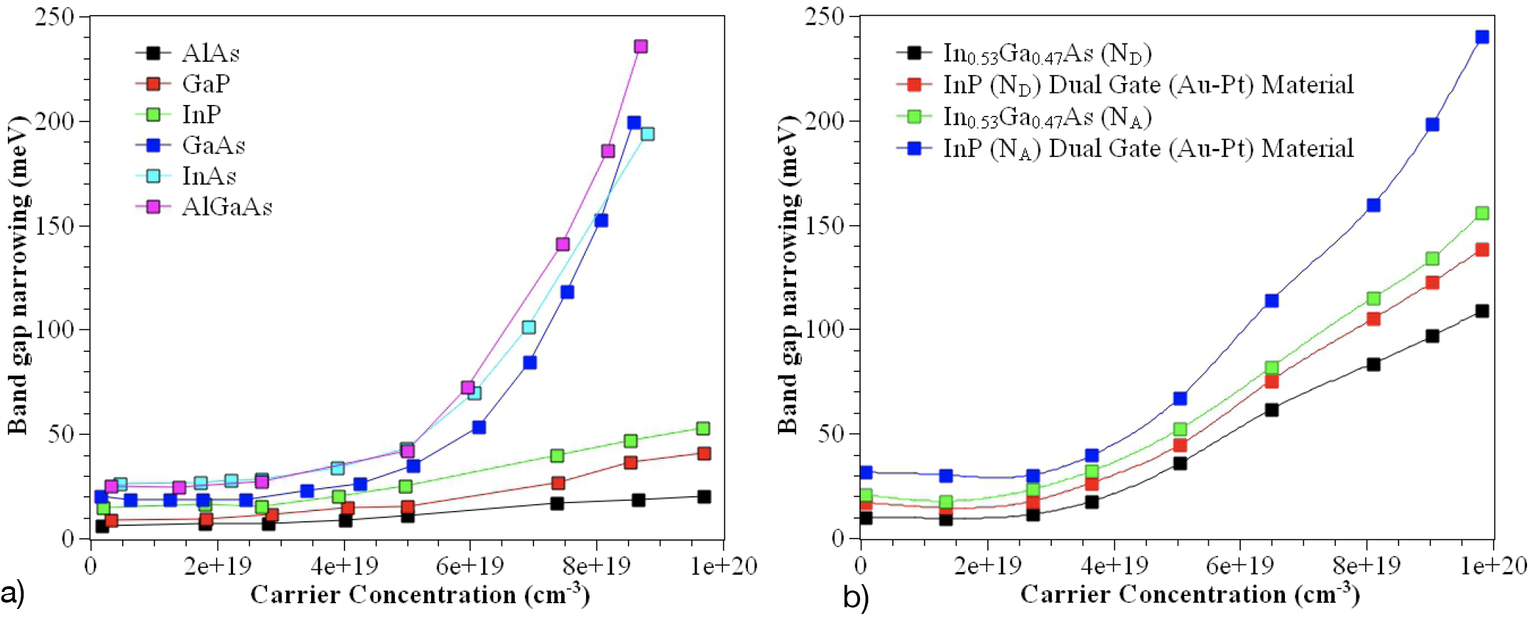
Figure 2. (a) Different Substrate Materials. (b) Dual Gate Material with conventional MOSFET model. Carrier concentration based on dual-gate (Au-Pt) material compared with previous research [1-3, 7].
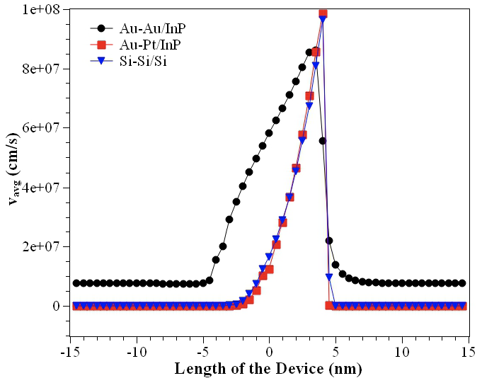
Figure 3. The mean velocity of electrons in the channel for different materials’ based devices.
.jpg)
Figure 4. (a) Comparison of electrostatic potential.
.jpg)
Figure 4. (b) Comparison of Transconductance values with the proposed work and [10].
The detailed analysis has been tabulated in Table I. From this, it can be concluded that the Gold and Platinum dual-gate material-based DG MOSFET provides a deeper and enhanced valley for high-speed operations. The average velocity of the electron in different materials is analyzed, and the results were compared. It describes that the electron velocity is higher in gold and platinum-based DG MOSFETs than in Si-Si based DG MOSFETs [11-13]. The comparisons of electrostatic potential and transconductance parameters have been shown in figure 4.
Conclusions and future aspects
Future nano-CMOS device structures are constructed using non-silicon materials to overcome the existing MOSFETs’ basic limitations. Materials such as InGaAs and AlxGa1-xAs come across recent research to create faster MOSFETs with more significant scalability factor. These materials have increased mobility of electrons. The gate had greatly influenced the channel potential. As a result of this, the Cylindrical Surrounding MOSFET model was not able to model accurately. Reducing the channel length by 40% can focus on creating the work in the CSDG paradigm.
This work mainly focuses on creating an illustration that is suitable for fully depleted CSDG MOSFETs. Furthermore, the work can be extended in developing the Cylindrical Surrounding Double-Gate (CSDG) MOSFETs with inert semiconductors materials and various other materials
References
[1] Juan Villa, Inigo Ramiro, Jose M. Ripalda, Ignacio Tobías, Pablo García-Linares, Elisa Antolin, and Antonio Martí, “Contribution to the study of sub-bandgap photon absorption in quantum dot InAs/AlGaAs intermediate band solar cells,” IEEE J. of Photovoltaics, vol. 11, no. 2, pp. 420-428, March 2021.
[2] R. J. W Hill, D. A. J Moran, X. Li, H. Zhou, D. Macintyre, S. Thoms, A. Asenov, P. Zurcher, K. Rajagopalan, J. Abrokwah, R. Droopad, M. Passlack, and I. G. Thayne, “Enhancement-mode GaAs MOSFETs with an In0.3Ga0.7As channel, a mobility of over 5000 cm2/Vs, and transconductance of over 475 μS/μm,” IEEE Electron Device Letters, vol. 28, no. 12, pp. 1080-1082, 27 Dec. 2007, 10.1109/LED.2007.910009.
[3] Dipanjan Sen, B. Goswami, A. Dey, P. Saha, and S. K. Sarkar, “Impact of self-heating and nano-gap filling factor on AlGaAs/GaAs junction-less DG-MOSFET based biosensor for early-stage diagnostics,” IEEE Region 10 Symposium, Dhaka, Bangladesh, 5-7 June 2020, pp. 662-665.
[4] Mojtaba Allaei, M. Shalchian, and F. Jazaeri, “Modeling of short-channel effects in GaN HEMTs,” IEEE Trans. on Electron Devices, vol. 67, no. 8, pp. 3088-3094, Aug. 2020.
[5] Xueqing Liu and M. S. Shur, “TCAD model for TeraFET detectors operating in a large dynamic range,” IEEE Trans. on Terahertz Science and Technology, vol. 10, no. 1, pp. 15-20, Jan. 2020.
[6] D. A. Firsov, I. S. Makhov, V. Y. Panevin, M. Y. Vinnichenko, L. E. Vorobjev, A. P. Vasil’ev, and N. A. Maleev, “Enhance of impurity related terahertz emission in optically pumped GaAs/AlGaAs quantum well structures,” 43rd Int. Conf. on Infrared, Millimeter, and Terahertz Waves (IRMMW-THz), Nagoya, 9-14 Sep. 2018, pp. 1-2, DOI: 10.1109/IRMMW-THz.2018.8509889.
[7] D. Stark, L. Persichetti, M. Montanari, C. Ciano, L. Di Gaspare, M. De Seta, M. Zoellner, O. Skibitzki, G. Capellini, M. Ortolani, L. Baldassarre, M. Virgilio, T. Grange, S. Birner, K. Rew, D. J. Paul, J. Faist and G. Scalar, “N-Type Ge/SiGe quantum cascade heterostructures for THz emission,” Conf. on Lasers and Electro-Optics Europe & European Quantum Electronics Conference (CLEO/Europe-EQEC), Munich, Germany, 23-27 June 2019, pp. 1-1, DOI: 10.1109/CLEOE-EQEC.2019.8872902.
[8] P. Schygulla, F. Heinz, D. Lackner, and F. Dimroth, “Subcell development for wafer-bonded III-V//Si tandem solar cells,” 47th IEEE Photovoltaic Specialists Conf., Calgary, Canada, 15 June – 21 Aug. 2020, pp. 2716-2719.
[9] Yu Qian Liu, Chang Chun Chai, Han Wu, Yu Hang Zhang, Chun Lei Shi, and Yin Tang Yang., “Mechanism of AlGaAs/InGaAs pHEMT nonlinear response under high-power microwave radiation,” IEEE J. of the Electron Devices Society, vol. 8, pp. 731-737, 2020.
[10] J. P. Colinge, FinFETs, and other multi-gate transistors, Springer, New York, USA, 2008.
[11] Viranjay M. Srivastava, “Scaling effect of cylindrical surrounding double-gate MOSFET: A device beyond 22 nm technology,” 4th Int. Conf. on Advanced Computing and Communication Systems, Coimbatore, India, 6-7 Jan. 2017, pp. 1-5.
[12] Viranjay M. Srivastava and G. Singh, MOSFET technologies for double-pole four throw radio frequency switch, Springer International Publishing, Switzerland, Oct. 2013.
[13] Naveenbalaji Gowthaman and Viranjay M. Srivastava, “Analysis of n-type double-gate MOSFET (at nanometer-scale) using high-K dielectrics for high-speed applications,” 44th Int. Spring Seminar on Electronics Technology, Spain, 5 – 7 May 2021, Accepted.
_Based_Double-Gate_MOSFET_for_High-Speed_Devices_-_POSTER.png)
Ilustration 1. Presented Poster at LAEDC 2021.
1 Department of Electronic Engineering, Howard College, University of KwaZulu-Natal, Durban, 4041, South Africa. Email: gowthamann@ukzn.ac.za https://orcid.org/0000-0002-7030-7919
2 Department of Electronic Engineering, Howard College, University of KwaZulu-Natal, Durban, 4041, South Africa. Email: viranjay@ieee.org https://orcid.org/0000-0001-5231-7403